Power Stage Design
To power the buffer and mixer opamps, the design will need a power stage that supports
- Bi-polar or symmetric voltage rails that will allow “rail-to-rail” positive and negative headroom for the +/- audio signal.
- Enough current for 5 (4 input + 1 mix) dual channel opamps.
The simplest method for creating a negative voltage rail is….tonot create a negative voltage rail! In other words: use a voltage divider to create DC bias mid-point at the positive voltage rail. This has the effect of level-shifting the operating point of the opamp so that the ground reference is halfway between 0 volts and the positive rail. This requires only passive components - which is cheap - but also complicates the opamp design and can create issues with the opamp behaviour itself. You also have to be careful to filter out the DC from the input and output to prevent “pops” and damage to other devices such as speakers. I’m not a fan for these reasons.
A better way is to actually create a new negative voltage rail from the existing positive rail.
You can do this easily with a charge pump voltage regulator. This is an inductorless topology - already a benefit - but has very limited current capabilities - usually only 10-40mA - and is unregulated. This means the generated negative voltage is easily pulled down by the load if it consists of more than a couple of opamps. In practical terms, you could require a charge pump circuit for each opamp channel. Its also recommended to put a passive low pass filter on each charge pump output to prevent ripple. Each charge pump circuit requires roughly 6 components. In total that could be lot of components when you multiply that per opamp, per channel.
In the end I settled on the Cuk regulator topology using the LM2611 converter IC. This is a buck-boost type regulator with an inverted output rail. And it comes in a tiny SOT-23 footprint!
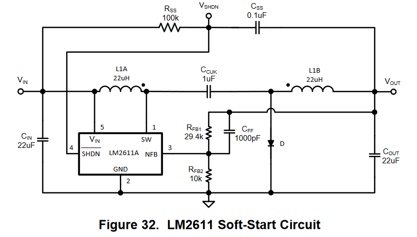
Here is the reference design from the datasheet.
Soft Start
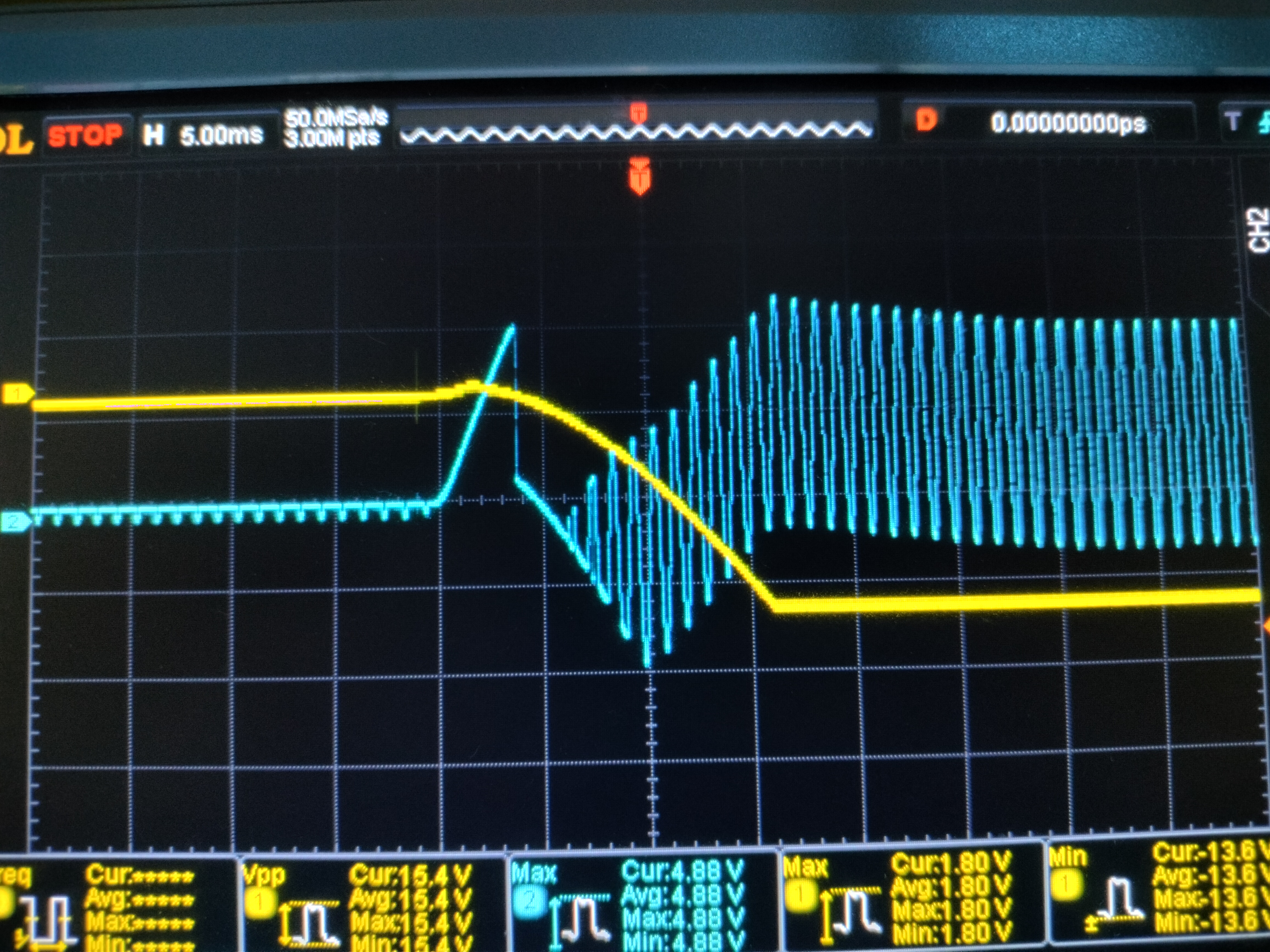
Since the IC doesn’t contain a soft-start feature, required additional circuitry is shown in the image above. Without the soft-start, the in-rush current will significantly exceed the current consumption specification. In fact, it tripped the lab power supply current protection; I thought the board had a short. I had to adjust the current protection to to more than 1 Amp to allow the circuit to power up correctly! Not great if you’re trying to prevent lab accidents. Adding the soft-start circuitry meant that the board powered up peaking at 60mA…which is a massive drop and far mroe acceptable. Below is a screenshot of the scope capture. Negative power rail from the LM2611 is Yellow, output signal is shown in Blue. The power rail is now much more gradual, rather than a sudden off-on transition. The datasheet implied there would still be a voltage spike at the peak of the turn on transtition but looking at the capture below, it would seem that the voltage spike with the soft-start has also been minimised greatly.
However, a large voltage spike remains on the output signal when the board is powered up. This is the culprit for the pop or thump you often hear in the output device speakers. Not sure what is the best solution here: Maybe caps on the output path, maybe delayed opamp start or maybe just turn the board on before any down stream amplifiers.
Output Voltage
The output voltage can be adjusted using the negative feedback resistors RFB1 and RFB2. Rather unhelpfully the datasheet did not contain the equation to calculate the resistor divider values. I found the equation on a post in the TI forums. Maybe this is EE101 but I can’t reconcile that omission in my head.
| VREF | RFB1 | RFB2 | VOUT |
|---|---|---|---|
| -1.23v | 2.2K | 22k | VREF * (1 + (RFB2/RFB1) = -13.5v |
Note, that the resistors must not exceed 50Kohm. According to the datasheet this is due to leakage at the NFB pin.
Using common resistor values it was only possible to reach just under 12v or quite a bit over. So I opted for the latter. Better to have a larger power supply swing than too little. It also gives some allowance for load regulation.
Current Draw and Load Regulation
The application curve from the datasheet shows that with -12V output, the max current it could provide would be 400mA.
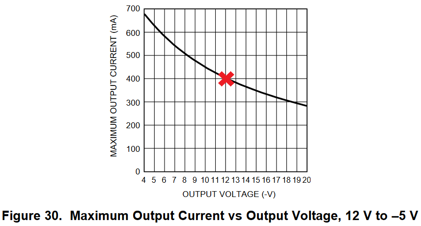
Bearing in mind the quiescent voltage of each TL072 opamp is only 1.2mA, this is overkill. However, during active use, the current will certainly be higher.
The datasheet boasts Better Regulation Than a Charge Pump but then fails to offer any evidence elsewhere in the datasheet. I have no doubt that this claim is broadly true - charge pumps have abysmal load regulation. However, I’m always sceptical about the claims of load regulation on these regulator IC’s. Usually when a company omits test results from the datasheet it’s because the results were not so great.
Below are the load regulation test results from 10mA to 400mA. Test was run using a TENMA 72-13210
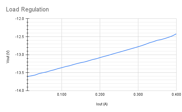
The negative voltage rail dropped by ~1.2V at the max load of 400mA, which is a 10% drop. That’s actually not too bad. Although if I had picked < 12V output I might not be so forgiving. Still, better than a charge pump…
Final note on the Cuk topology: There don’t appear to be many IC’s out there that support this type of regulator. Either it’s overlooked or it has some major drawback that I’m missing here.
I noticed later it is possible to create an inverting regulator from a synchronous buck regulator. See this app note from TI. However, there are significant limitations:
- the input voltage needs to be higher than the minimum required voltage for the device
- The maximum allowable output voltage is limited by the maximum Vdev minus the maximum input voltage.
- The maximum load current cannot be more than the maximum current through the internal switches.